Quick. What's the world's most expensive attack submarine?
Hint: it costs as much as a nuclear aircraft carrier, and it's so expensive that the very wealthy government that purchased it can barely find the money to build two more submarines in this class.
Give up?
Well, it's the U.S. Navy's Seawolf attack submarine, SSN21, which cost over US$1 billion to build.
Quick. What microprocessor is used in the computer system that runs this impressive undersea vessel's combat data systems? (Remember, the U.S. Navy pulled out all the stops to make this the most potent attack submarine on the face of the earth.)
Intel Corp.'s Pentium II?
Nope, Intel has its hands full supplying the PC market with microprocessors, why does it need government business?
Hint: it's made by Motorola Corp.
A PowerPC 604?
Nope. Another hint: it's a member of an old line of CISC microprocessors.
An MC68060?!
Getting close, now go back two generations.
An MC68030?!!!!!!
Bingo! The USS Seawolf's Lockheed Martin BSY-2 system, which runs the ship's combat data systems, is based on a network of some 70 or so 68030 Motorola processors. (Don't believe it? Well, just go to the Naval Technology Web site and read about the submarine for yourself.)
That's right, this impressive submarine on which the U.S. government spared no cost, has a combat data systems computer system based the same microprocessor that powered the Macintosh Classic II, a personal computer so old that most Macintosh enthusiasts wouldn't consider it for any serious use other than as a doorstop.
But why?
Absolutely elementary--the most important term in the above description is not the designation of the microprocessor, it's the word "network." That's right, a computer system based on a network of cheap, low-power microprocessors can outperform, and at the same time offer greater reliability and easier performance upgrading, than a system based on a single high-performance microprocessor. This is something the U.S. government has known for a long time, and a fact that Be Inc. recently discovered, which is why the Be operating system is drawing so much interest. Want to double the performance of your personal computer? Don't throw out your present computer and buy a new one; just buy a cheap card with another CPU on it and double the size of your memory.
Of course, another reason for using an "old microprocessor" is the fact that it takes software engineers a lot longer--usually two or three times as long--to harness the full computing power of a microprocessor than it takes the hardware engineers to design and manufacture the chip. This is because the software engineers have to learn the hardware architecture (particularly if they plan to write program code in "assembly language"), then they have to design and write the source code, debug it (bugs dramatically increase in number as the amount of code increases) and test it, optimize the code to make sure it runs quickly, and finally document it. In other words, writing good software, which is something the U.S. government is likely to insist on for a highly sophisticated submarine, is a long and involved process.
On the other hand, the way personal computers for civilian use are developed is completely different, since personal computers are usually built around a single microprocessor. Accordingly, in order to double system performance, which is normally evaluated in terms how many millions of instructions per second (MIPS) the central processing unit can process, it is necessary to develop a completely new microprocessor. This is a job that due to competition for market share is done at breakneck speed in 18 months or so. Unfortunately, this fast development cycle occasionally leads to errors in chip design that can sometimes affect even simple arithmetic calculations, which may be another reason the U.S. government is satisfied with older chips for newer ships!
Once the microprocessor development cycle is finished, sample chips are sent out to personal computer systems makers who incorporate them into new personal computer designs. The designing and development of a new personal computer system can be done in about six months, although it could take a little longer. Once completed, sample personal computer systems are sent out to software houses to get them started on software development--and that's when the problems begin. This is because the development of new operating systems and software applications for new computer hardware, whether it is for government or civilian use, takes--as noted above--two or three times as long as hardware development.
So what's the result? Well, to begin with, new versions of operating systems are always late. Both of the leading personal computer operating system developers, i.e., Microsoft Corp. and Apple Computer Inc., have regularly produced new operating systems and version upgrades behind schedule, although for some inexplicable reason only Apple Computer has been lambasted by the press for its performance in this area. Moreover, since third party software developers can't begin development of application software packages until they have at least a developer's release of the new operating system, they have to wait until most of the bugs are worked out of the new operating systems, which as noted above takes more and more time as the amount of code increases--and have operating systems for personal computers been growing in size!
After the third party application developer gets a developer release of the new operating system whose stability it can trust, and which hopefully runs faster than the older version, it has to develop a new software application within the shortest possible time as a result of market forces (e.g., the operating system developer's software applications division may have already begun development on the same type of application). Accordingly, niceties such as thorough debugging and testing are out, and making the documentation as brief as possible is a big plus that can speed things up. Moreover, optimization for high-speed running is great in theory, but since memory capacity doubles in size with every new computer system, things should work well enough until there's a chance to do an upgrade, for which, needless to say, the consumer will be charged an "appropriate fee."
Now, at this point, the clever reader is probably thinking, not without good reason, that the whole personal computer development cycle is being dictated by the hardware developers, who have a shorter development cycle than software developers and don't give a damn if it results in sloppy, bloated software for end users. So, the clever reader might be asking himself/herself, why doesn't someone develop the operating system first and then develop a microprocessor to support it afterward? And to make things better, why not design the microprocessor so that it can be easily networked with other microprocessors, and hence get all the benefits of networking?
Welcome to the world of the TRON VLSI CPU!
The TRON VLSI CPU architecture is a 32-bit microprocessor architecture that was developed expressly for serving as the "main hardware building block" of the real-time TRON Hypernetwork (called the highly functional distributed system [HFDS] in technical parlance), which is the ultimate goal of the TRON Project. Inside this hypernetwork, the overwhelming majority of the computer systems will be so-called "intelligent objects," that is, the computerized appliances and machinery that fill human habitations and workspaces. In an HFDS that encompasses a country, for example, there would literally be billions of these intelligent objects. Accordingly, the TRON VLSI CPU specification had to describe a general-purpose microprocessor architecture with real-time enhancements that could readily be applied to embedded systems in addition to personal computers and workstations, and it had to embody state-of the-art microprocessor technology as it existed in the mid 1980s when the architecture was laid down. The main characteristics of the resulting TRON VLSI CPU architecture can be summarized as follows:
There have been several technically successful implementations of the TRON VLSI CPU architecture by Japanese electronics makers that offer good performance (see below), and the resulting microprocessors have been incorporated into everything from appliances and machinery to large-scale, non-stop transaction servers. However, in spite of the fact that it's an open architecture that can be freely cloned, TRON VLSI CPU-specification microprocessors were never adopted by foreign electronics makers, and they never really made it in large numbers to the desktop. Why is this? Well, at approximately the same time the TRON VLSI CPU architecture was being drawn up, a new movement to speed up the on-chip processing of microprocessors used in desktop systems was taking place in the U.S. This led to a new design philosophy for microprocessor chips that moved away from the design approach that the TRON VLSI CPU architecture is based on. Let's take a moment to explain these two design approaches.
The computer systems that surround us today are based on an architectural prototype model called SISD, which stands for single instruction single data stream. This is also called the von Neumann architecture. In this type of a computer system, a single central processing unit (usually a microprocessor) operates across a common bus (instruction/data pathway) in conjunction with a main memory (usually dynamic random access memory [DRAM] chips), where instructions and data are stored while the system's power supply is on. When program instructions are executed, the microprocessor takes the instructions from the memory and executes them using "registers" (temporary storage locations) built inside it. Although there are many factors involved, the speed of this type of computer system basically depends on the speed of the bus, the speed of the main memory, and the amount of time it takes the processor to execute the instructions.
The biggest bottlenecks in this architectural prototype have traditionally been the width of the bus (the wider the better), the capacity and access time of the main memory, the clock speed of the microprocessor (measured in megahertz), and the number of registers available on the microprocessor (the more the better). In early computer systems, such as 8-bit and 16-bit personal computers, main memory capacity was originally only 64 kilobytes and 256 kilobytes, respectively. This is just a tiny fraction of what is available in today's 32-bit personal computers. As a result, computer designers traditionally tried to develop compact program code (i.e., the object or machine code of zeroes and ones that the microprocessor actually processes) to reduce the number of instructions that would sit in the memory and move across the bus. To do this, they built long, complex instructions onto the microprocessor chip in the form of "microcode," which supported the constructs of the high-level languages that programs are written in.
However, the solution to the bottleneck problems created a new problem, and the biggest problem with this traditional architectural design model, which later came to be known as "complex instruction set computer," or CISC, was the size of the instruction sets. In fact, some CISC designs have as many as 200 instructions in microcode. These huge instruction sets take up a lot of room on the chip, which reduces the amount of room for registers and other devices. Moreover, as a result of their length, the complex instructions are executed very slowly. That is to say, it can take many "machine cycles" to execute a single complex instruction.
As a solution to the performance problems of the CISC approach, a new approach to the design of microprocessor architecture, called "reduced instruction set computer," or RISC, came into being. RISC designs were proposed much later when high-capacity memory was available at low cost and 32-bit microprocessor designs were being implemented. The RISC design approach is a result of studies on the efficiency of CISC designs, which progressively became more difficult to speed up and took longer to develop. These studies showed that only a tiny portion of the on-chip instructions are normally used in a program, and that their varying lengths made execution time slow. Accordingly, they proposed using much smaller instruction sets (which are not in microcode on the chip; some RISC chips operate with as few as 34 instructions), in which each instruction is of the same length (32-bits), and hence can be executed extremely rapidly, that is, in a single "machine cycle." The smaller instructions sets also made it possible to add many more registers, and they made it easier to incorporate peripheral devices such floating point units and high-speed cache memory onto the microprocessor chip. Moreover, the lack of on-chip microcode made it possible to raise clock speeds of microprocessors dramatically.
Of course, the RISC approach is not all pluses and no minuses. There are several disadvantages that come with the RISC approach, which are: (1) compiling and debugging program code for a RISC machine requires a very large, sophisticated compiler, which is difficult to develop; (2) the size of the object code of programs (the machine code the computer actually processes) is considerably larger than that for the CISC approach, which means the the main memory must be larger; (3) high-speed cache memory usually has to be used in one or more levels between the processor and the main memory because of the great difference in speed between the processor and the main memory; (4) the system bus must be comparatively faster due to the fact that there is more object code to send across to the processor; and (5) all these high speed operations generate a lot of heat, which, depending on the system, may require the use of cooling fans. Perhaps most problematic of all from the view of the TRON Project is the fact that the performance gains obtained by using RISC designs mainly benefit the applications, not the operating system.
Although the design team working on the TRON VLSI CPU architecture knew about the pluses and minuses of the RISC approach, they had to take other factors into consideration, such as software productivity and the wider range of targeted computer systems, most of which would be embedded systems. The RISC engineers by comparison had an advantage in that they could focus their attention entirely on desktop systems where there are fewer constraints on system design. Accordingly, the TRON VLSI CPU architecture stuck with the tried and tested CISC approach, which it brought to a high level of refinement while incorporating as many advanced microprocessor features as possible.
So what is the TRON VLSI CPU architecture like?
The TRON VLSI CPU architecture, like just about everything else in the TRON Architecture, is divided into "levels." These are:
Bare minimum to satisfy the TRON VLSI CPU specification (i.e., <<L1>> minus some high-level instructions)
Implementation without MMU (i.e., <<L1>> minus MMU support instructions)
99 basic instructions
| Data transfer | 8 |
| Comparison, test | 3 |
| Arithmetic | 15 |
| Logical | 4 |
| Shift | 6 |
| Bit manipulation | 5 |
| Fixed-length bit field | 6 |
| Variable-length bit field | 4 |
| BCD arithmetic | 4 |
| String manipulation | 4 |
| Queue manipulation | 3 |
| Control transfer | 12 |
| Multiprocessor support | 3 |
| Control space, address space | 8 |
| OS-support | 8 |
| MMU support | 6 |
In addition to these 99 basic instructions, there are an additional 22 coprocessor and 11 decimal arithmetic instructions.
Extensions and planned features (e.g., INDEX)
Planned specification for expansion to 64-bit operation
Alternative implementations of TRON VLSI CPU specification features (e.g., control register handling)
Implementation of something not in specification (e.g., instructions to interface with in-circuit emulator)
Although the TRON VLSI CPU architecture specifies the above six levels, certain aspects of microprocessor design, such how to design the memory management unit (MMU) and the translation look-aside buffer (TLB), or how many pins should be placed at the at the bottom of the chip package are left up to each company implementing the architecture.
For people who are not very familiar with microprocessor architecture, the 99 instructions listed above may seem like a considerable number, particularly in comparison to early RISC designs. However, this is a considerable smaller instruction set in comparison to the one used for Intel Corp.'s 80x86 microprocessor series, which is used to power the ubiquitous IBM-PC clones. In fact, that architecture, which like the TRON VLSI CPU uses on-chip microcode, recently had 57 new instructions added to it for processing multimedia data. Intel refers to these instructions as MMX technology, and it just licensed the technology to competitors such Advanced Micro Devices Inc. Moreover, the main alternate to the Intel architecture, the PowerPC "RISC architecture" developed by IBM and Motorola for use in Apple Computer Inc.'s Macintosh personal computer line, has more than 100 instructions, and chances are that it will also pick up new instructions for multimedia to compete with the Intel architecture. So it should be stressed here that the TRON VLSI CPU architecture is a well-thought out, elegant instruction set for a CISC design that is neither too big nor too small. On top of that, it's very efficient.
How efficient? Let's consider the following two examples in which ITRON OS-oriented high-level instructions incorporated in the Gmicro/100 microprocessor are used in place of low-level instructions.
First, let's consider the use of the following "queue instruction (insert to a doubly linked queue)," which is used to improve processing efficiency in manipulating the ready queue employed in task switching in real-time processing. It requires 12 bytes of code to write and 18 machine cycles to process.
QINS @(R1,FOR)<@(RDQ_TBL,R2*8)
However, if the same instruction is written with a combination of simple instructions a la RISC approach, we end up with 36 bytes of code that take 26 machine cycles to process.
MOV     @(RDQ_TBL+4,R2*8),Rn
MOV     R1,@(RDQ_TBL+4,R2*8)
MOVA    @(RDQ_TBL,R2*8),@(R1,FOR)
MOV     Rn,@(R1,BACK)
MOV     R1,@(Rn,FOR)
The result is that this high-level instruction allows for processing is carried out in roughly one half the time, while at the same time realizing a two-thirds reduction in code size.
Let's take another example--the "bit search (search for bit in variable-length bit field)" below, which is used by the task scheduler in a real-time operating system to find the highest-priority task. When we use this instruction, we end up with 14 bytes of code which are processed in 62 machine cycles.
MOVA    @RBQ_BIT,R0
MOV     #0,R1
MOV     #272,R2
BVSCH/F/1
However, when we attempt to accomplish the same thing with low-level instructions, which is what would be done on a RISC chip, we end up with 78 bytes of code that require 244 machine cycles to process.
                 MOVA       @RDQ_BIT,R0
                 MOV        #0,R1
                 MOV        #0,R2
                 MOV        #7,R3
                 MOV        #0,R4
     SRCH1:      CMP.W      #0,@R0
                 BNE        FOUND1
                 ADD        #1,R0
                 ACB        #1,R1,#8,SRCH1
     FOUND1:
     SRCH2:      CMP.B      #0,@R0
                 BNE        FOUND2
                 ADD        #1,R0
                 ACB        #1,R2,#3,SRCH2
     FOUND2:     MOV.B      @R0,R4
                 MOV.W      #H'FE,R5
     SRCH3:      AND.B      R5,R4
                 BEQ        FOUND3
                 SHL.B      #1,R5
                 SCB        #1,R3,#0,SRCH3
     FOUND3:     SHL        #5,R1
                 SHL        #3,R2
                 ADD        R2,R1
                 ADD        R3,R1
In this case, the result of using the high-level instruction is that processing takes place in one quarter of the time, while the amount of code required decreases by 82 percent.
Accordingly, it can be seen that the TRON VLSI CPU architecture is a superb architecture for real-time embedded applications, which is the main purpose it is suppose to serve in the TRON total architecture.
The history of the TRON VLSI CPU architecture goes back to a Microcomputer Software Applications Experts Committee at the Japan Electronic Industrial Development Association, which was set up in the early 1980s to investigate the relationship between microprocessors and future real-time operating systems. The decision to develop a new standard microprocessor architecture was made in part because existing microprocessor designs were burdened by the need to maintain compatibility with past designs, thus slowing them down. Another problem was openness. After licensing their 8-bit and 16-bit microprocessor designs to Japanese semiconductor companies in order to create "world standards," U.S. semiconductor companies cut off access 32-bit microprocessor designs, so that they could enjoy the fruits of monopoly markets. Thus there was a tremendous need for an open 32-bit microprocessor architecture that Japanese companies could apply their semiconductor manufacturing expertise to.
The first TRON VLSI CPU-specification microprocessor to hit the market was the Gmicro/200 (10 MIPS/20MHz), which appeared in January 1988. This chip was the first in a family of five microprocessors based on the TRON VLSI CPU architecture that have been jointly developed to date by Hitachi Ltd., Fujitsu Ltd., and Mitsubishi Electric Corp. In addition to the microprocessor itself, three peripheral chips, an interrupt request controller (IRC), a direct memory access controller (DMAC), and a tag memory (TAGM), were simultaneously announced, to which a floating point unit (FPU) was added in December 1988.
In August 1988, Toshiba Corp. announced the TX1 (12.5 MIPS/25MHz), along with with a peripheral chip, the TX ICT, which is an interrupt controller/timer. Unlike the three companies mentioned above, which aimed at pooling their resources to produce a full-line of TRON VLSI CPU-specification microprocessors to cover all possible uses, Toshiba had its sights set on using TRON VLSI CPU-specification microprocessors for embedded use and as an application specific integrated circuit (ASIC) core. Hence, microprocessors in the TX series do not have MMUs.
In August and November of 1989, the Gmicro/100 (10 MIPS/20MHz) and Gmicro/300 (20 MIPS/20MHz) were respectively announced. The former, like the TX1, was intended for use in real-memory systems, that is, for embedded use. The latter, like the Gmicro/200, includes an MMU, and thus can be used as the CPU for a workstation. In fact, both of these chips were incorporated into the MCUBE "pure BTRON" workstations marketed by Personal Media Corp. The latest version of the MCUBE based on the Gmicro/300 uses the BTRON3 operating system, which is specially designed to take advantage of the high-level instructions on the TRON VLSI CPU-specification microprocessor. The Gmicro/300 also made it into a non-stop transaction processor called the Sure System 2000, which was developed and marketed by Fujitsu.
The Gmicro/100 was turned into an application-specific standard product (ASSP) in May 1990, the year in which the Gmicro group also announced another important peripheral chip, the cache controller memory (CCM) to support the Gmicro family. May 1990 also saw the announcement of Matsushita Electric Industrial Co.'s MN 10400 (20 MIPS/20MHz), which like Toshiba's TX1 and the Gmicro group's Gmicro/100 is intended for embedded use, and hence does not incorporate an MMU.
Oki Electric Industry Co. took the TRON VLSI CPU architecture in another direction when it announced its O32 microprocessor (15 MIPS/33MHz) in November 1990. This implementation has special features that support its application in fault-tolerant systems, such as equipment used in non-stop telecommunications networks.
The Gmicro/300 received a speed boost in April 1991, when a 33MHz version was announced. Interestingly, this microprocessor, which is in the middle of the Gmicro family, has appeared in more more versions--with clock speeds of 20MHz, 25MHz, 33MHz, and 40MHz--than any other TRON VLSI CPU-specification microprocessor, which indicates that it has been selected for use in a wide variety of systems.
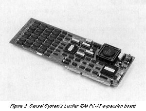
In February of the following year, 1992, the most outstanding addition to the Gmicro family's peripheral chip line-up, the Gmicro vector processing unit (VPU), was announced (Fig. 1). This peripheral chip is literally a supercomputer on a chip; it has a peak performance of 206 MFLOPS (million floating point operations per second) at 50MHz (single-precision floating point arithmetic), which gives Gmicro-based workstations the capability to do scientific and engineering calculation on a par with the latest workstations.
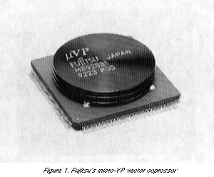
Note: For those who have difficulty understanding how fast 206 MFLOPS is, Intel Corp. caused quite a stir in the late 1980s when it unveiled its 80860 processor, which it called a "Cray supercomputer on a chip." That chip, which was later used as a coprocessor in Intel-based personal computers, could do 66 MFLOPS at 33MHz. The 33MHz version of the Gmicro VPU can do 136 MFLOPS (single-precision floating point arithmetic)! The Gmicro VPU, like the 80860 before it, was later incorporated into an expansion board IBM PC-AT personal computers. This was developed and marketed in Japan by Sansei System Ltd. (Fig. 2).
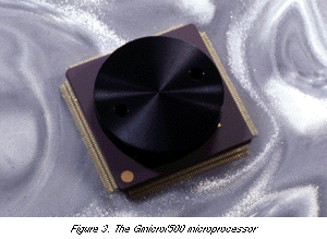
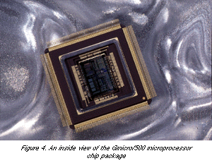
In May 1993, Toshiba announced TX2 (25 MIPS/25MHz), which the company considers the ideal core for ASIC/ASSP applications. Among its advanced features are a power saving function that reduces power consumption to one-tenth of normal while it is in the WAIT mode. Also in 1993, the Gmicro group announced the Gmicro/500 (130 MIPS/66MHz), which is currently the fastest and most capable of the microprocessors based on the TRON VLSI CPU architecture (Figs. 3 and 4). In addition, the Gmicro group announced a study aimed at developing an advanced version of the Gmicro/100, the Gmicro/400, in 1994.
Unlike memory chips, such as DRAMs, microprocessors require software to support development and testing, and, in the case of an open architecture such as the TRON VLSI CPU architecture aiming at "object code compatibility," a validation suite to assure that software can be ported from one chip to another. Accordingly, from the beginning of the chip subproject, participating Japanese semiconductor firms have been in contact with specialist firms overseas to have compilers and software development environments prepared for 32-bit microprocessors based on the TRON VLSI CPU architecture. These include Green Hills Software Inc. and Microtec Research Inc.
The latest C language compiler for the Gmicro family, for example, has been optimized and now includes global register allocation, loop invariant code motion, loop unrolling, loop merging, and elimination of tail recursion. As for assuring object compatibility, a validation suite has been developed for testing chips that do not employ virtual memory (implementation level <<L1R>>); it tests 26 addressing modes, 82 instructions, and 10 kinds of exceptions, interruptions, and traps (EIT).
So what's the future of the TRON VLSI CPU and microprocessors based on it?
At this point in time, it seems like the TRON VLSI CPU-specification microprocessors have firmly secured a place for themselves in the world of embedded applications, and thus will probably continue to be utilized as cores for ASICs and ASSPs. In fact, as noted above, a TRON VLSI CPU-specification microprocessor is better suited for this field than a RISC-based microprocessor, because the size of the object code of the programs it runs is considerably smaller than that for a RISC-based chip. In fact, four of the eight implementations of the TRON VLSI CPU, the TX1, TX2, Gmicro/100, and MN 10400, are aimed squarely at the embedded systems market. Thus there is a very good chance that a TRON VLSI CPU-specification chip could enter your home one day incorporated into some consumer appliance manufactured by a Japanese electronics maker.
On the other hand, as for desktop systems, it does not look like TRON VLSI CPU-specification microprocessors, or other CISC-based microprocessors for that matter, are going to survive the race to supply human personal computer end users with the dramatic increases in computing power that they have become accustomed to receiving every year. This is because there are two big disadvantages with CISC-based designs: (1) they take longer to develop, and (2) they are costlier to manufacture. Thus, as long as desktop personal computers continue to be built around a single microprocessor, microprocessors based on the RISC scheme have the advantage and will most likely to take over the market for desktop systems.
Basic information on the TRON VLSI CPU architecture and microprocessors based on it can be obtained from the annual proceedings of the TRON Project symposia. The majority of the papers on the TRON VLSI CPU-specification chips appeared between 1987 and 1991. The proceedings were published by Springer-Verlag from 1987 to 1990, and have been published by the IEEE Computer Society Press since 1991.
A description of the TRON VLSI CPU architecture can also be found in the April 1987 issue of IEEE Micro, which is a special issue on the TRON Project.
The technical specifications for the TRON VLSI CPU architecture can be obtained from the TRON Association, whose address is as follows: